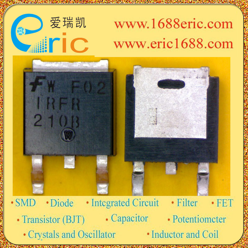
IRFR210BTF-FP001 FR2108 的参数 |
| 最大源漏极电压Vds
Drain-Source Voltage |
200V |
| 最大栅源极电压Vgs(±)
Gate-Source Voltage |
|
| 最大漏极电流Id
Drain Current |
2.7A |
| 源漏极导通电阻ΩRds
DΩ/Ohmain-SouΩ/Ohmce On-State Ω/Ohmesistance |
1.5Ω/Ohm @1350mA,10V |
| 开启电压Vgs(th)
Gate-Source Threshold Voltage |
2.0-4.0V |
| 耗散功率Pd
Power Dissipation |
2.5W |
| Description & Applications |
200V N-Channel MOSFET General Description These N-Channel enhancement mode power field effect transistors are produced using Fairchild’s proprietary, planar, DMOS technology. This advanced technology has been especially tailored to minimize on-state resistance, provide superior switching performance, and withstand high energy pulse in the avalanche and commutation mode. These devices are well suited for high efficiency switching DC/DC converters, switch mode power supplies, DC-AC converters for uninterrupted power supply and motor control. ? 2.7A, 200V, RDS(on) = 1.5? @VGS = 10 V ? Low gate charge ( typical 7.2 nC) ? Low Crss ( typical 6.8 pF) ? Fast switching ? 100% avalanche tested ? Improved dv/dt capability |
| 描述与应用 |
200V N沟道MOSFET 概述 这些N沟道增强型功率场效应晶体管都采用飞兆半导体专有的,平面的,DMOS技术。 这种先进的技术,特别是针对已尽量减少对通态电阻,提供出色的开关性能,并承受高能量脉冲在雪崩和减刑模式。 这些器件非常适用于高效率开关DC/ DC转换器,开关电源,DC-AC转换器,不间断电源和电机控制。?2.7A,200V,RDS上) =1.5Ω@ VGS= 10 V ?低栅极电荷(典型7.2nC) ?低Crss(典型6.8 pF) ?快速开关 ?100%雪崩测试 ?改进的dv / dt能力 |
| 技术文档PDF下载 |
在线阅读  |